Progress & Achievements

System concept, design, and modelling

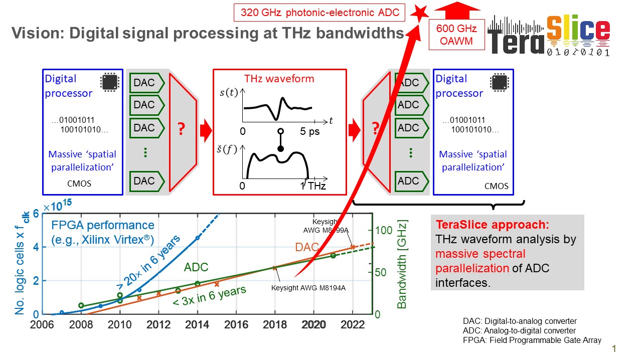
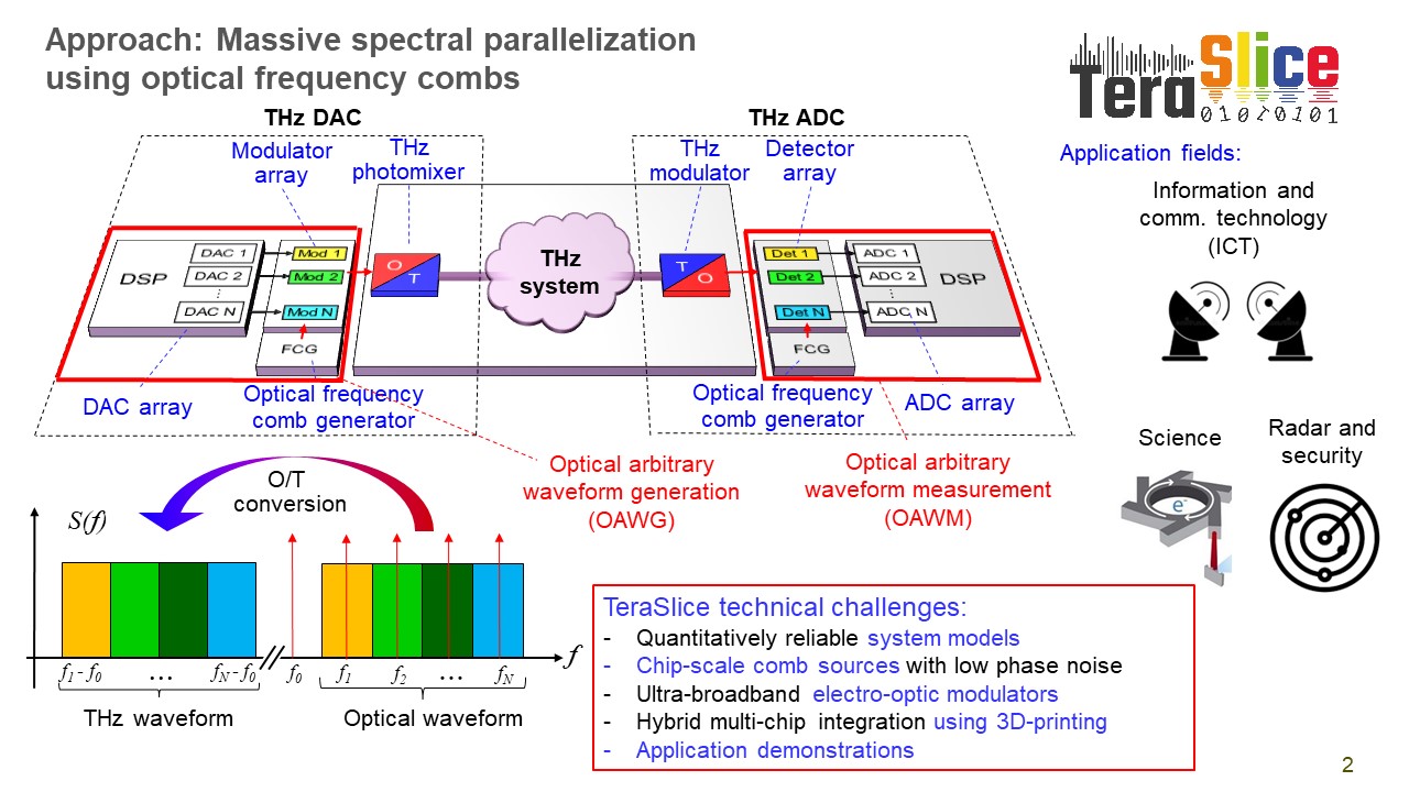
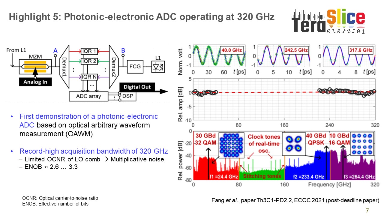
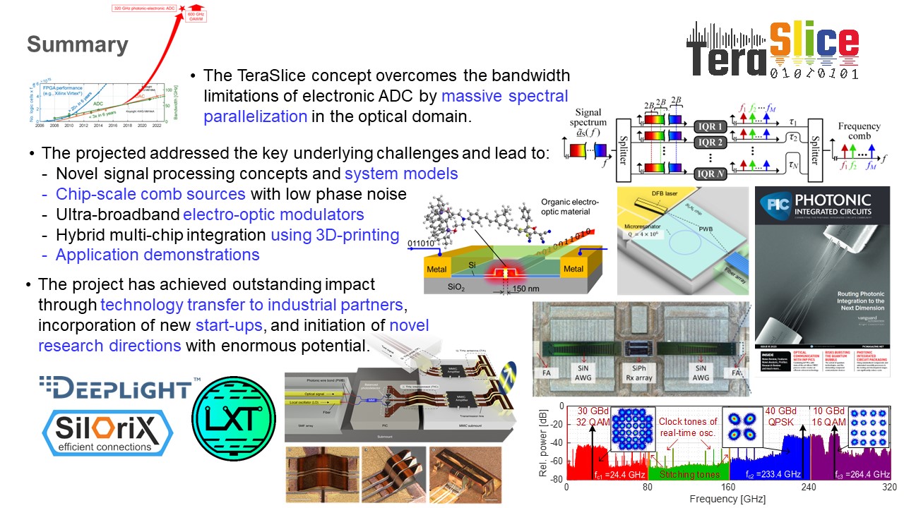
During the first 12 months, the complete architecture of the photonic ADC system has been defined and a theoretical model with additional simulations were made by THA and CNIT respectively, predicting key performance such as spurious-free working region (SFWR), spurious-free dynamic range (SFDR) and effective number of bits (ENOB). The overall architecture selected for the first-generation photonic ADC demonstrator (320GHz ADC), is reported in Fig. 1.

Fig. 1 – Architecture of the first-generation photonic ADC demonstrator

The specifications and characteristics of each constituting building block have been considered by THA for setting up a simple analytical model, in order to provide an overview of the expected performance of the demonstrator. For now, only one architecture is considered (320 GHz bandwidth, homodyne detection), but other versions (i.e. 1 THz bandwidth) can be easily extrapolated. The scalability of the concept will be assessed later during the project. In parallel, a system-level numerical simulation has been performed by CNIT, whose main result consists of identifying the abovementioned SFWR and SFDR performance (Fig. 2).

Fig. 2 – Evolution of signal voltage (blue square) reaching the scope (see Fig. 1) together with total noise floor (pink triangle) and highest spurious contribution (red square).

Ultra-broadband electro-optic modulator

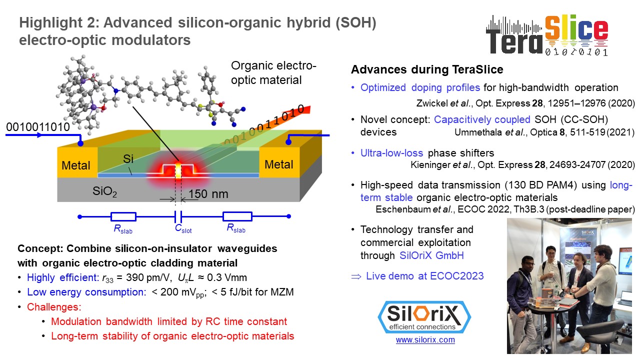
To realize an ultra-broadband electro-optic modulator for translating incoming THz waveforms onto an optical carrier, KIT investigated several possible approaches for combining the main key features such as large bandwidth, high modulation efficiency and low insertion loss. KIT designed and fabricated novel plasmonic-organic-hybrid (POH) modulators with the goal of minimizing the insertion loss (characterization in early 2021). In parallel KIT also investigated both resistively-coupled silicon-organic hybrid (RC-SOH) Mach-Zehnder Modulators (MZMs), showing theoretical bandwidth up to 200 GHz and losses below 0.5 dB. Fabrication of those devices is currently taking place by an external foundry with characterization scheduled on spring-summer 2021. The second approach relies on capacitively-coupled SOH (CC-SOH) modulators, which exploit a novel concept based on a THz slot-line to overcome the RC-related bandwidth limitations of the conventional RC-SOH devices. Experimental measurements (Fig. 3) demonstrate 3dB electro-optical bandwidth of 76 GHz and 1.3V·mm modulation efficiency.

Fig. 3 – Capacitively-coupled SOH MZM performance.(Left) Measurement of the π-voltage showing the intensity-modulation at the device output (red) for a low-frequency triangular drive signal (green). (Right) Dynamic behavior of a 1-mm-long CC-SOH MZM: the red curve shows the electro-optic (EO) response S21. As a reference, we also derive the EO response from the measured electrical S-parameters of the device using an analytical model [2] (blue curve).

Optical slicing filters

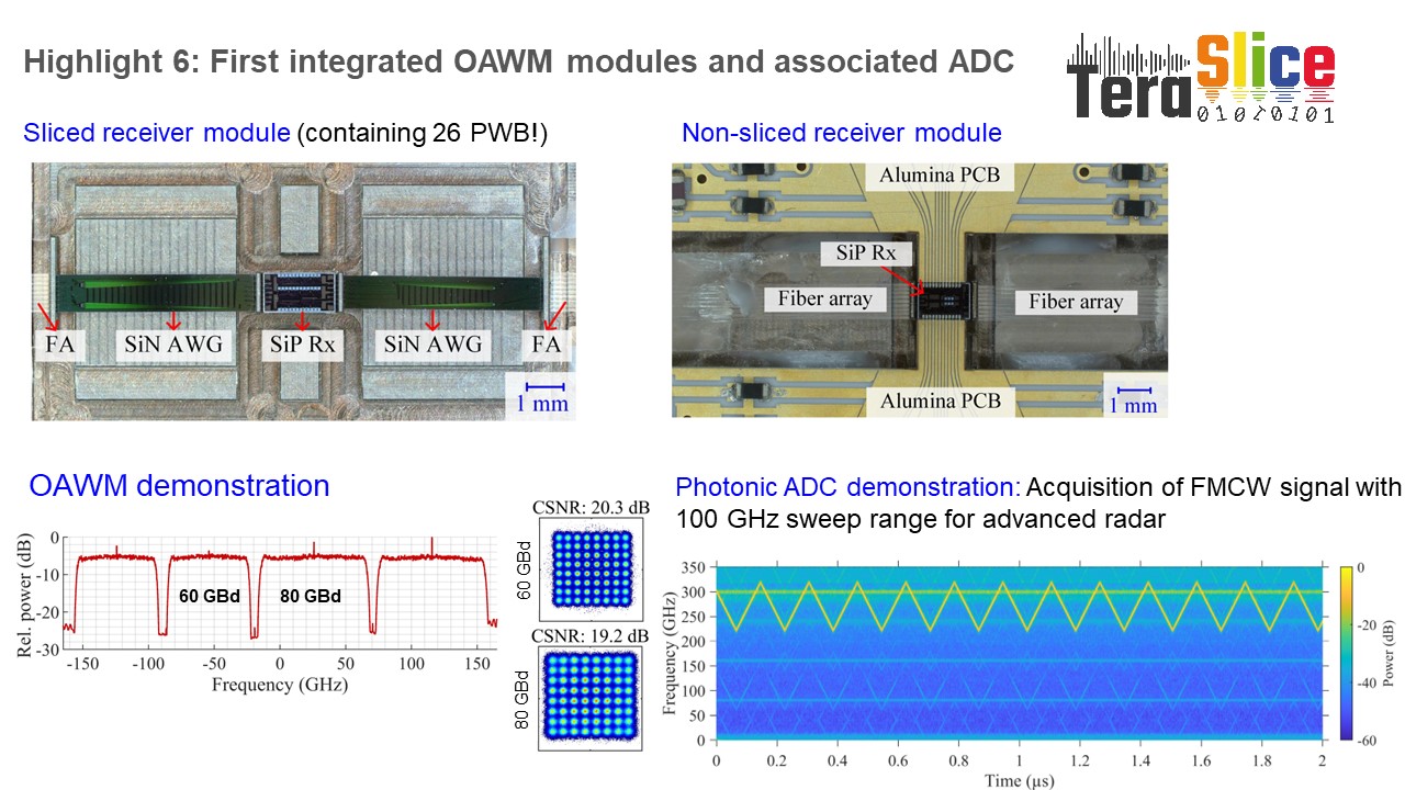
The spectral slicing filters were implemented by arrayed waveguide gratings (AWG). Simulations and preliminary tests are underway to determine whether LGT could perform the fabrication as required for the TeraSlice demonstration. If the outcome is positive, the system integration would benefit from having everything on one platform fabricated by LGT.  See Fig. 4 for the layout of one of the AWG filter designs.

Fig. 4 – Layout of an AWG filter for spectral slicing.

In the context of the first fabrication run, KIT also designed a filter for flattening the local oscillator (LO) comb tones, which relies on a cascade of ring filters – the layout of one of the implementations is shown in Fig. 5. In this layout, all LO comb lines are combined on the same waveguide leading to Output 2. Output 1 is used for extracting a portion of the residual pump tone, onto which the THz signal may be modulated.

Fig. 5 – Layout of the cascaded ring resonators for comb line selection and flattening.

An alternative design by CNIT on SiN for spectral comb line selection is currently underway, based on a micro-ring resonator-loaded Mach-Zehnder interferometer (MRR-MZI), which exhibits the potential of a higher rejection of adjacent lines and robustness to free-spectral range (FSR) mismatch between comb source and filter design, thanks to the squared spectral shaping.

Slice detector array

The sliced signal tributaries are coherently received by in-phase/quadrature (IQ) detectors, which we integrated on the silicon photonic platform. To this end, KIT has started a test run for a detector array with four parallel coherent receivers. Two alternative designs were sent to two different Silicon Photonics foundries, whose structure designs conceived with the main aim of mitigating the risk of fabrication errors. In both designs the bandwidth of balanced photodiodes is expected to be 40GHz.

Fig. 6 – One of the two layout of the IQ detector array sent for fabrication.

Both grating couplers and edge couplers as optical coupling interfaces were included for fiber arrays and photonic wire bonds (PWB) to allow both rapid testing of the devices and later integration into a chip-scale assembly. The chips are expected to be delivered in March 2021.

Comb generation

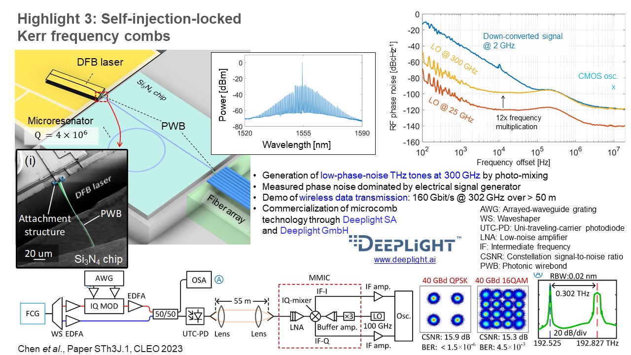
During the first 12 months, EPFL efforts focus on the development of a low-phase-noise Kerr comb generator. EPFL performed numerical simulations, designed and fabricated photonic integrated circuits with SiN microresonators, bus waveguides and integrated heaters. The fabricated devices with 40 GHz and 50 GHz free-spectral range (FSR) have been characterized, matching the required specifications. A single soliton microcomb using external-cavity diode laser (ECDL) with Erbium-doped fiber amplifier (EDFA) as a pump source was generated, providing the required 8 spectral modes with power per line >-22 dBm. Phase noise performance of the self-injection locked laser has been studied, together with the soliton microcomb repetition rate and noise multiplication for comb lines. 16 chips were sent to KIT matching the specification for the ADC experiment and photonic wire bonding. The chips containing ring resonators with requested FSR were designed and fabricated using LIGENTEC process (800nm SiN thickness), which allows to obtain high Q-factors and access to properly engineered dispersion. The layout included two (2) stand-alone chips of 5x5mm area (see Fig. 7); each of them contains ring resonators of 40 or 50 GHz FSR, with parameter sweep (ring radii, coupling gaps) around expected optimal values; all the rings have integrated heaters on top to allow thermo-optical tuning. The layout was optimized to fit the maximum number of ring variations and to ensure compatibility with standard equipment.

Fig. 7 Layout of the chips designed by LIGENTEC and EPFL, fabricated by LIGENTEC and delivered to KIT after testing.

Fig. 8 – (a) Optical spectrum of single soliton state. (b) Optical power of the first 8 comb lines (-22 dBm, 6 µW). Deviation is less than 1.5 dB; (c) Soliton repetition rate single at 39.772 GHz; (d) SSB Phase noise of soliton repetition rate, revealing low noise state.

EPFL has developed a robust packaging technique to build a compact module for photonic chip-based devices with high-power handling capability. This was possible thanks to a high mode confinement due to the high thickness of Si3N4 (~ 1 µm) and the use of a 2-cm-long ultrahigh-numerical-aperture (UHNA) fiber of 4.1 µm mode field diameter, to mode-match the fiber mode to the inverse taper’s mode on the Si3N4 chip facet. The industrial 14-pin butterfly packaging has built-in TEC and thermistor to control the microresonator temperature. It allows for wire bonding of the on-chip piezoelectric actuator. The transmission from input to output fiber is 15%.

Fig. 9 – Photonic packaging Si3N4 microresonator with input and output UHNA fibers and wire-bonding to integrated piezoelectric actuators.

Multi-chip assembly

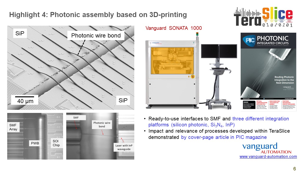
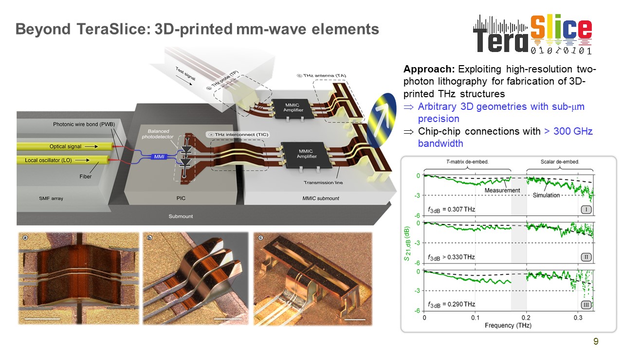
The first generation of the photonic wire bond processes was developed by VA, allowing optical connections between the different photonic platforms present in the project. A schematic of the planned assembly is depicted in Fig. 10.

Fig. 10 – Schematic of the planned TeraSlice assembly with different photonic circuits (in grey) and electrical circuits (green) which have to be connected. Depicted in red are the optical connections, realized via photonic wire bonds.

For a theoretical understanding of the different interface properties, a simulation environment for photonic wire bonds was set up with the commercial software Lumerical. Photonic wire bond processes at each interface were optimized separately on test chips. The optimization was done on a test assembly with a fiber connection to facilitate measurement of the connection. The following assemblies were used to develop and characterize the first generation of optical interfaces:

  • Fiber to photonic SiN chip
  • Fiber to photonic SOI chip
  • Fiber to laser

For the fiber to SiN connection test chips from LIGENTEC were used, containing loopback waveguides. Losses around 2 dB per photonic wire bond could be achieved. An image of a photonic wire bond between fiber and SiN chip and the corresponding measurement is shown in Fig. 11.

Fig. 11 – (Left) Microscope image of a photonic wire bond between a single mode fiber and a SiN chip. (Right) Optical transmission spectrum of one photonic wire bond, connecting a single mode fiber to a SiN test chip. The overall insertion loss is around 2 dB.

Development and testing of algorithms for digital reconstruction

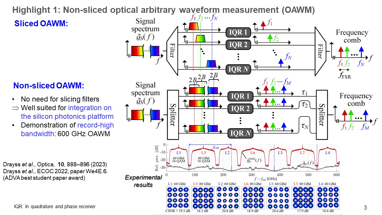
A mathematical description of the signals throughout the photonic ADC system, including distinction among time-invariant and time-variant signal impairments has been made by KIT. A system calibration process for retrieving the time-invariant part of the system transfer function was conceived and tested, based on the use of a highly stable optical pulse source. The further step was to estimate and compensate the time-variant impairments by using the spectral overlap region between adjacent spectral slices from the measurement itself. DSP algorithms have been implemented to stitch all the slices, removing time delays and amplitude/phase imbalances between the slices.

Test of the DSP algorithms in a proof-of-concept down-scaled photonic ADC experiment has been performed by KIT, where an 80 GBaud QPSK signal was sliced into four 20 GHz slices with subsequent spectral stitching digitally to recover the original signal.

Fig. 12 – Proof-of-concept experiment. (a) Four sliced spectrum of an 80 GBd QPSK signal. (b) Spectrum of the overlap region between slice 2 and slice 3. (c) wrapped phase (orange), unwrapped phase (blue) and linear fitting of the unwrapped phase (red) for the overlap region between slice 2 and slice 3.

Fig. 13 – Constellation for the reconstructed 80GBaud data signal.

References

[2]    J. N. Kemal et al., “32QAM WDM transmission at 12 Tbit/s using a quantum-dash mode-locked laser diode (QD-MLLD) with external-cavity feedback,” Opt. Express, vol. 28, no. 16, pp. 23594–23608, Aug. 2020, doi: 10.1364/OE.392007.