TERASLICE focuses on 3 key research breakthroughs:
-
-
- Establish a novel class of ultrabroadband electro-optic modulators using capacitively-coupled silicon-organic hybrid (SOH) devices, enabling conversion to the optical domain of RF signal with analogue bandwidths of up to the Terahertz range.

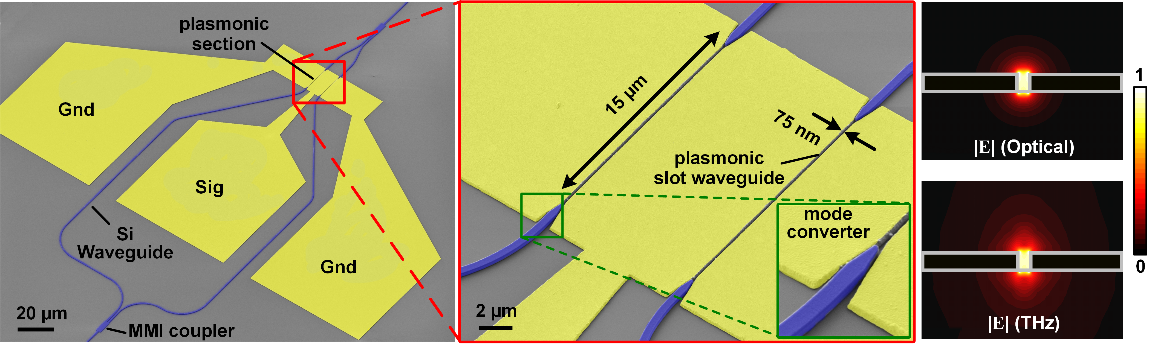
Plasmonic-organic hybrid (POH) modulator structure fabricated at KIT
- Establish chip-scale dispersion-engineered soliton microcomb generators based on ultrahigh-Q silicon nitride (SiN) resonators, with ultra-low pump power levels and superior coherence properties.

A Si3N4 microcomb system in a compact package, realized at EPFL
- Develop optical coupling concepts with low back-reflection and high-power handling capability. The system is realized as a photonic multi-chip assembly that combines the distinct advantages of different integration platforms such as Indium Phosphide (InP), silicon photonics (SiP) or SiN. Photonics wire bonds, facet-attached micro-lenses and edge-coupling interfaces will be all considered.

REM picture of photonic wirebond demo-connections realized at Vanguard Automation
- Establish a novel class of ultrabroadband electro-optic modulators using capacitively-coupled silicon-organic hybrid (SOH) devices, enabling conversion to the optical domain of RF signal with analogue bandwidths of up to the Terahertz range.
-
A first theoretical and numerical modelling step will lead to the design of the system, enabling at the same time performance prediction of spectral parallelization of ADC interfaces and investigate scalability of the approach for interfaces with analogue bandwidths of up to 1 THz.
TERASLICE, through the realization of final system-level demonstrators, aims at demonstrating both the operation capabilities of the photonic ADC and the advantages deriving from its effective use in specific application fields. A first-generation of photonic multichip modules (MCM) for ultra-broadband ADC, including custom RF packaging will be achieved and include the use of algorithms for digital reconstruction of the THz signal including digital signal processing for spectral stitching of signals, to be developed, implemented and experimentally verified along the project. A second-generation TERASLICE photonic ADC will be eventually embedded in application scenarios such as spectrum sensing and radar, for benchmarking and performance evaluation.
The work plan of TeraSlice is shown in the figure below, with the mutual interactions highlighted among the activities and the type of activity.
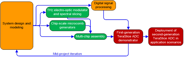
The work plan of the activities of TeraSlice, with in orange the numerical and/or theoretical activities, in green the technological development activities and in red the planned system-level demonstrations
The overall concept that is developed in TERASLICE is shown in the figure below. An analogue THz signal is transferred to the optical domain using an ultra-broadband electro-optic modulator. Optical demultiplexing filters are used to spectrally slice the optical signal into a multitude of band-limited components that can be coherently detected using an array of in-phase/quadrature (IQ) receivers along with a chip-scale optical frequency comb generator that provides a multitude of phase-locked local oscillator (LO) tones as precise phase references. The outputs of the IQ receivers (IQR) are fed to a parallel array of synchronized ADC, and the original electromagnetic signal can be reconstructed from the ADC outputs by digital signal processing (DSP).
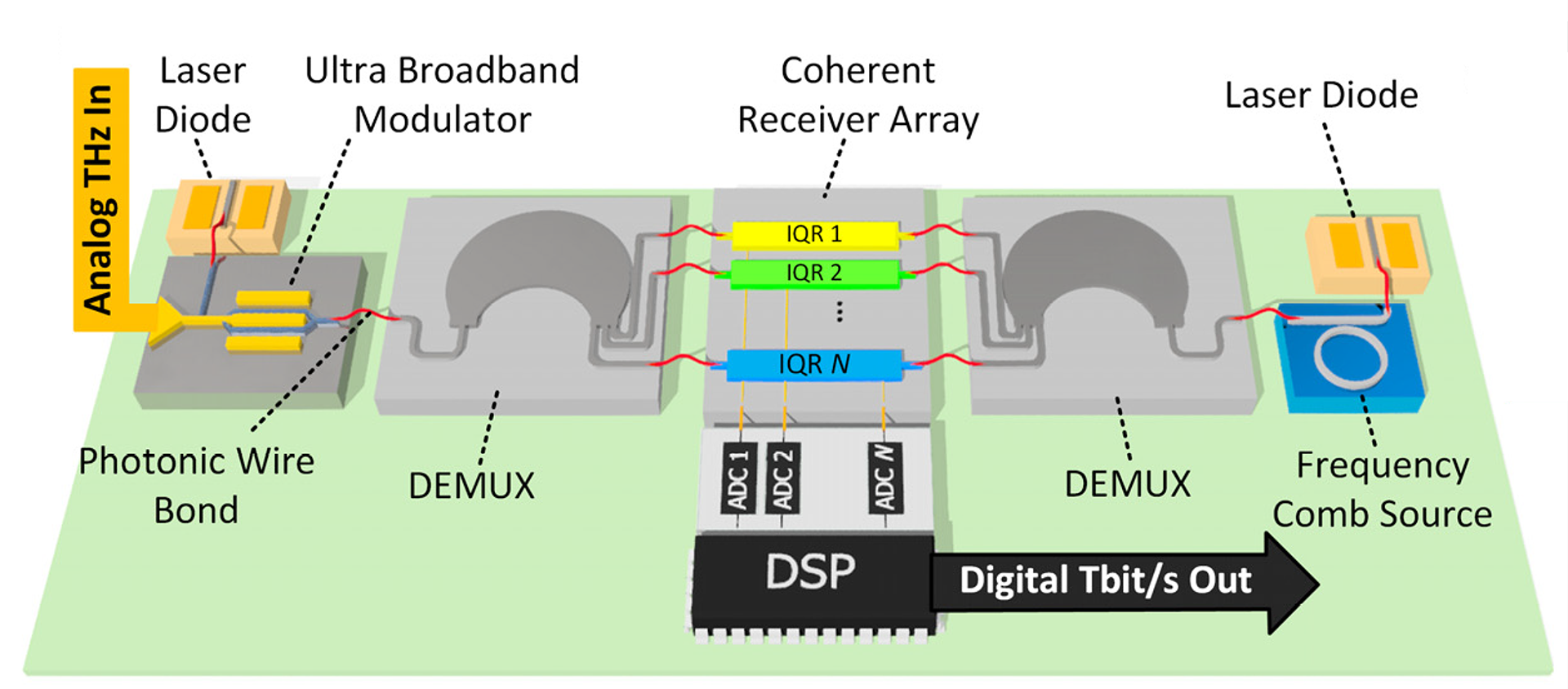
Technological concept of the chip-scale ultra-broadband photonic analogue-to-digital converter (ADC), offering scalability to THz bandwidths by massive spectral parallelization in the optical domain.