System concept, design, and modelling
The complete architecture of the photonic ADC system has been defined and a theoretical model with additional simulations were made by THA and CNIT respectively, predicting key performance such as spurious-free working region (SFWR), spurious-free dynamic range (SFDR) and effective number of bits (ENOB). The overall architecture selected for the first-generation photonic ADC demonstrator (320GHz ADC), is reported in Fig. 1.
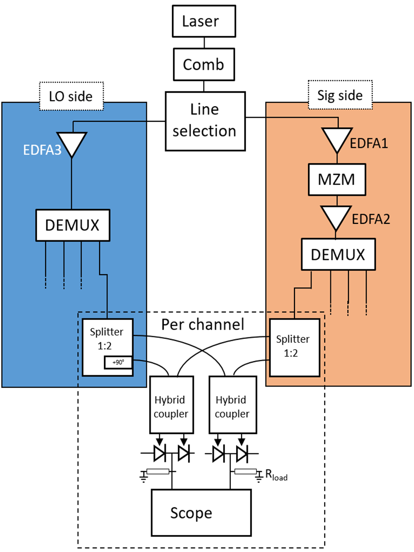
Fig. 1 – Architecture of the first-generation photonic ADC demonstrator
The specifications and characteristics of each constituting building block have been considered by THA for setting up a simple analytical model, in order to provide an overview of the expected performance of the demonstrator. For now, only one architecture is considered (320 GHz bandwidth, homodyne detection), but other versions (i.e. 1 THz bandwidth) can be easily extrapolated. The scalability of the concept will be assessed later during the project. In parallel, a system-level numerical simulation has been performed by CNIT, whose main result consists of identifying the abovementioned SFWR and SFDR performance (Fig. 2).
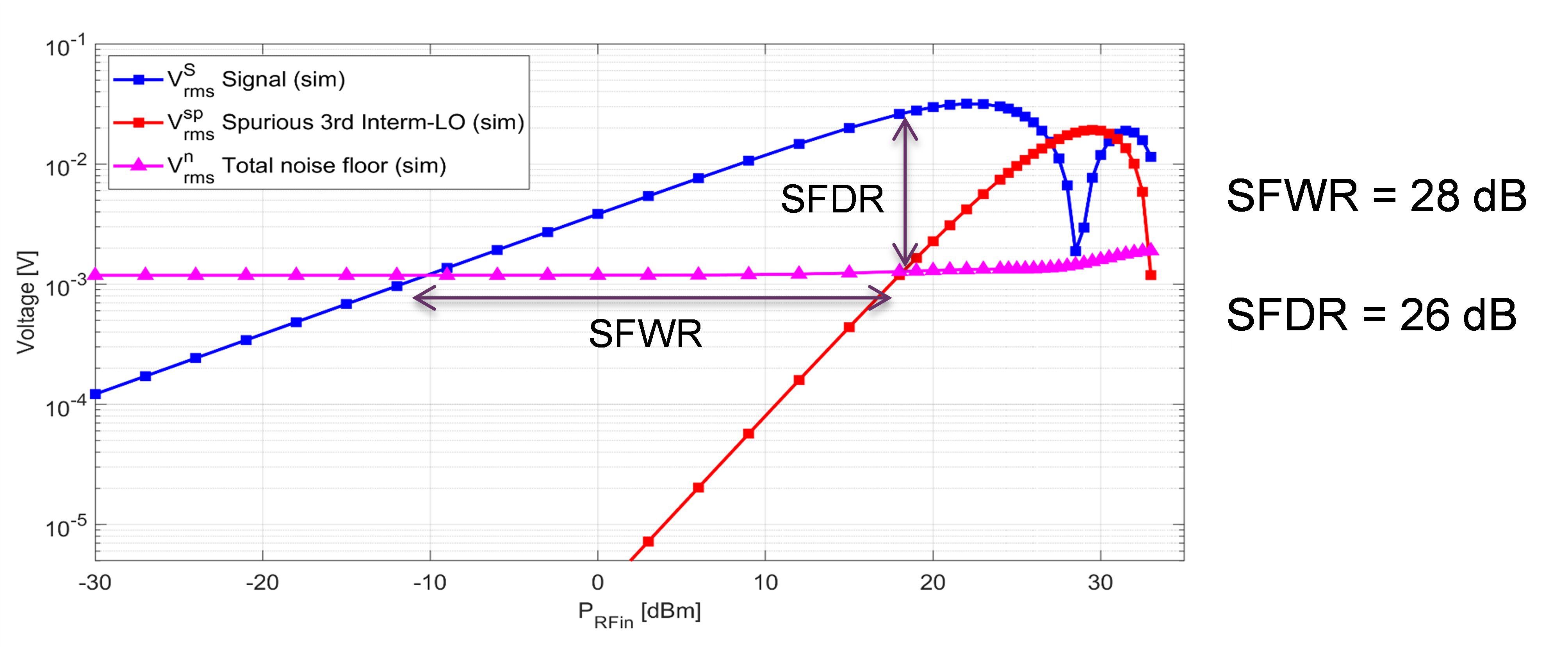
Fig. 2 – Evolution of signal voltage (blue square) reaching the scope (see Fig. 1) together with total noise floor (pink triangle) and highest spurious contribution (red square).
First experimental results led to model and simulation refinement. Using the analytical model, the different voltage contributions detected on oscilloscope were estimated, and compared to the experimental values. This includes the signal of interest at 2 GHz, spurious signals generated by the Mach Zehnder modulator (MZM), oscilloscope (ADC) and optical noise (mainly amplified spontaneous noise ASE and thermal noise). Figure 2.2 shows that the model and the experimental results are in good agreements. The optimal Signal to Noise and Distortion ratio (SINAD) is around 17 dB both experimentally and in the model. We see that, in both case, SINAD is limited by the ASE noise at low RF power, and by the MZM non-linearity at higher RF powers. Extrapolations for a signal at 320 GHz were made taking into account the loss of efficiency of the MZM at that frequency. SINAD is estimated to be reduced by 2 dB compared to low frequency.
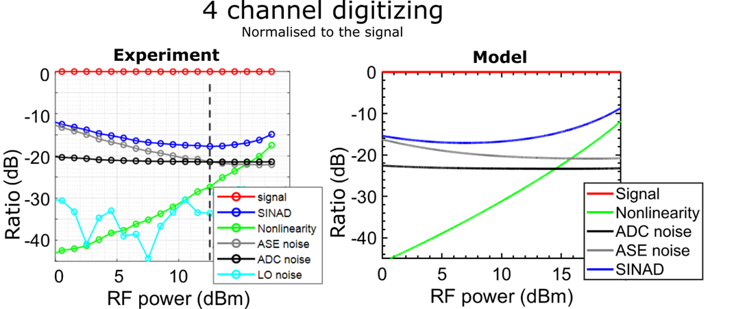
Figure 2.2. Comparison between model and experiment for a RF frequency of 2 GHz.
Ultra-broadband electro-optic modulator
To realize an ultra-broadband electro-optic modulator for translating incoming THz waveforms onto an optical carrier, KIT investigated several possible approaches for combining the main key features such as large bandwidth, high modulation efficiency and low insertion loss. KIT designed and fabricated novel plasmonic-organic-hybrid (POH) modulators with the goal of minimizing the insertion loss (characterization in early 2021). In parallel KIT also investigated both resistively-coupled silicon-organic hybrid (RC-SOH) Mach-Zehnder Modulators (MZMs), showing theoretical bandwidth up to 200 GHz and losses below 0.5 dB. Fabrication of those devices is currently taking place by an external foundry with characterization scheduled on spring-summer 2021. The second approach relies on capacitively-coupled SOH (CC-SOH) modulators, which exploit a novel concept based on a THz slot-line to overcome the RC-related bandwidth limitations of the conventional RC-SOH devices. Experimental measurements (Fig. 3) demonstrate 3dB electro-optical bandwidth of 76 GHz and 1.3V·mm modulation efficiency.
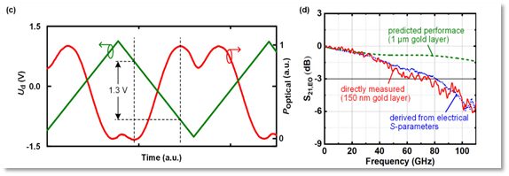
Fig. 3 – Capacitively-coupled SOH MZM performance.(Left) Measurement of the π-voltage showing the intensity-modulation at the device output (red) for a low-frequency triangular drive signal (green). (Right) Dynamic behavior of a 1-mm-long CC-SOH MZM: the red curve shows the electro-optic (EO) response S21. As a reference, we also derive the EO response from the measured electrical S-parameters of the device using an analytical model [2] (blue curve).
Optical slicing filters
As a second set of key components, the TeraSlice concept relies on filters for slicing the signal and LO spectrum in the spectrally slices scheme and for separating and spectrally flattening the tones of the LO. The spectral slicing filters were implemented by using arrayed waveguide gratings (AWG). The simulations and designs with different channel spacings were carried out by KIT, see Figure 4 for the layout of one of the AWG filter designs. These AWG filters were fabricated by the LGT on the silicon-nitride (SiN) platform. After a few iterations of design, fabrication, and characterization by KIT, the specified performance was achieved. The measured transmission of four pairs of AWG filters with good alignment in frequencies are shown in Figure 5. The measured channel spacing and free spectral ranges (FSR) match very well with the designed values of 80 GHz and 400 GHz respectively. The insertion loss of the LO AWG filters is approximately 2.5 dB, while the signal AWG filters exhibit higher insertion loss of approximately 6 dB.
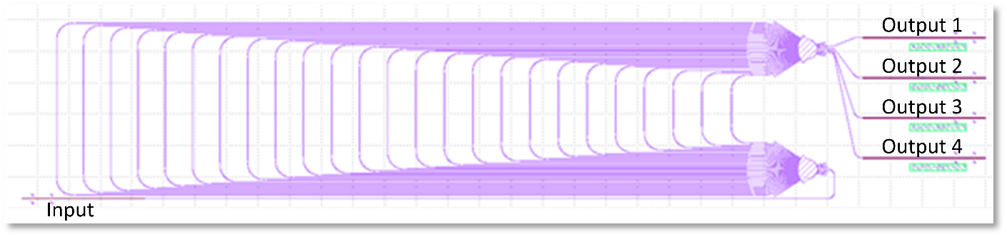
Fig. 4 – Layout of an AWG filter for spectral slicing. The incoming broadband optical waveforms are fed in to the Input port and sliced into four tributaries that are emitted at the Output ports.
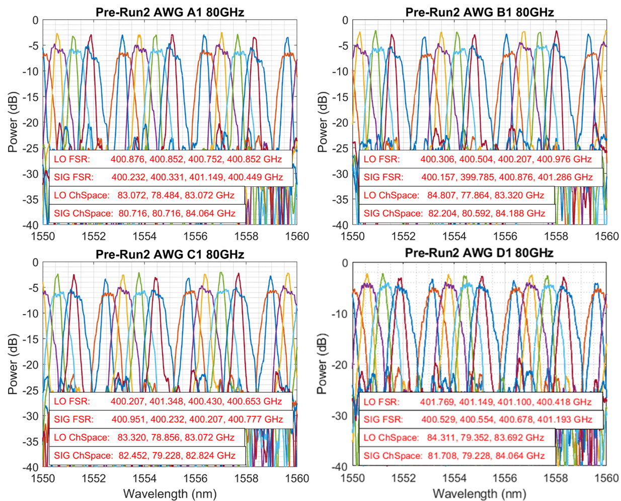
Fig. 5 – Measured transmission characteristics of four pairs of frequency-aligned AWG filters for signal slicing and LO-comb separation. The measured channel spacing and free spectral range (FSR) match very well to the designed values of 80 GHz and 400 GHz respectively.
KIT has also designed filters for flattening the LO comb tones, based on a cascade of ring filters. The layout of one of the implementations is shown in Figure 5.1. For the final goal of a 320 GHz photonic-electronic ADC demonstration, the FSR of the LO comb should be 40 GHz. Our design objective was hence to achieve low loss while maintaining high suppression at 40 GHz. To achieve this goal, we vary the coupling gap between the bus waveguide and the rings in our design within the range of 0.3 µm to 0.6 µm with an increment of 0.1 µm. The transmission of the single ring filter is then measured, and the resulting curve is fitted with a Lorentzian function, as shown in Figure 5.2(a). From these curves, we extract the excess loss and the suppression at 40 GHz. In Figure 5.2(b), we plot these values against the coupling gap. Our findings indicate that the best trade-off between low loss and good suppression at 40 GHz occurs within coupling gaps ranging from 0.4 µm to 0.5 µm.
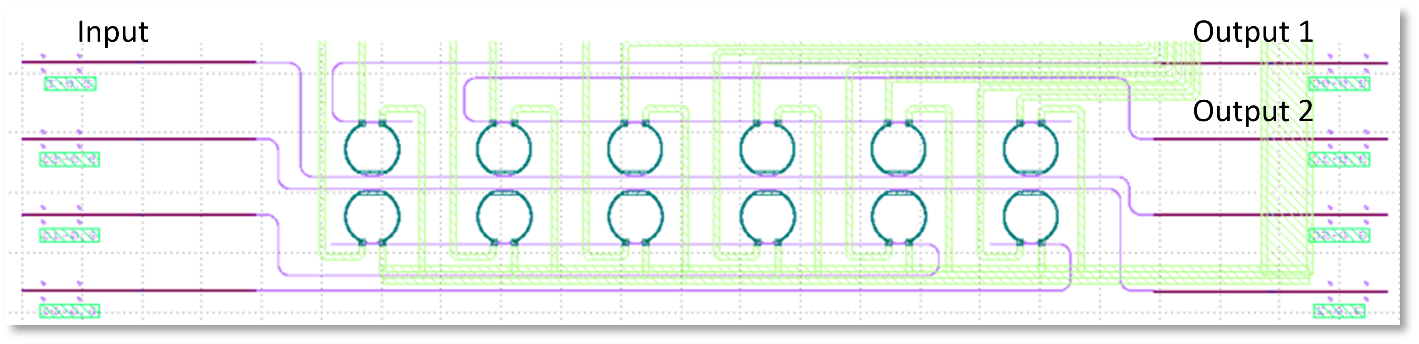
Fig. 5.1 – Layout of a cascaded ring resonators for comb line selection and flattening. In this layout, all LO comb lines are combined on the same waveguide leading to Output 2. Output 1 is used for extracting a portion of the residual pump tone, onto which the THz signal may be modulated.

Fig. 5.2 – (a) Transmission curves for the single ring filter with different coupling gaps between the bus waveguide and ring structure. (b) The extracted insertion loss as a function of coupling gap. (c) Suppression at 40 GHz as a function of coupling gap.
Slice detector array
The sliced signal tributaries are coherently received by in-phase/quadrature (IQ) detectors, which we integrated on the silicon photonic platform. To this end, KIT has started a test run for a detector array with four parallel coherent receivers. Two alternative designs were sent to two different Silicon Photonics foundries, whose structure designs conceived with the main aim of mitigating the risk of fabrication errors. In both designs the bandwidth of balanced photodiodes is expected to be 40GHz.
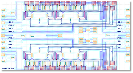
Fig. 6 – One of the two layout of the IQ detector array sent for fabrication.
Both grating couplers and edge couplers as optical coupling interfaces were included for fiber arrays and photonic wire bonds (PWB) to allow both rapid testing of the devices and later integration into a chip-scale assembly. The chips are expected to be delivered in March 2021.
Comb generation
EPFL efforts focused on the development of a low-phase-noise Kerr comb generator. EPFL designed and fabricated photonic integrated circuits with Si3N4 microresonators,
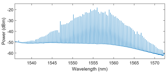
bus waveguides and integrated heaters. The fabricated devices have been characterized, matching the required specifications in terms of free-spectral range (FSR) 39.7-40.2 GHz range. A single soliton microcomb using an external-cavity diode laser (ECDL) with a single sideband modulator and Erbium-doped fiber amplifier (EDFA) as a pump source was generated, providing the required 8 optical with power per line >-22 dBm and OSNR of >30 dB. Also using the undercoupled microresonator we obtained single soliton and multisoliton states using DFB self-injection locking technique at 270-400 mA DFB current corresponding to 70-100 mW optical power. By carefully adjusting the parameters of the laser self-injection: feedback phase, and DFB current one can achieve a single soliton state. OSNR for 8 comb lines is up to 29 dB as depicted in Figure 7.
EPFL has also developed a generic packaging technique to build a compact module for photonic chip-based devices using fibers. The critical feature that distinguishes our packaging technique from other solutions is the high-power handling capability, which is central for optical microresonator applications. The numerical aperture of output waveguides is much higher than for single-mode fibers. Using SMF fibers spliced with UNHA-7 fiber we performed packaging of the photonic chip-based microresonator. The industrial 14-pin butterfly packaging has a built-in TEC and thermistor to control the microresonator temperature. The transmission from input to output fiber is up to 20%. Such a packaged unit containing a D70_11 chip and glued input and output fibers was sent to KIT for the main ADC experiment
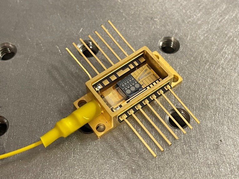
Fig. 7
Multi-chip assembly
Within TeraSlice the optical interconnects for the multi-chip assemblies are realized with photonic wire bonds. Photonic wire bonds (PWB) are single-mode freeform waveguides fabricated with additive 3D nanofabrication that efficiently connect integrated optical chips to each other.
Generic interface processes for PWB connection of various optical elements of the TeraSlice multi-chip assemblies such as PICs based on indium phosphide, silicon-on-insulator, silicon nitride and single mode fibers were developed and optimized within the project. Figure 8 shows an image of a PWB between an SOI chip and a single mode fiber array. Those processes for the individual interfaces could then be combined with great flexibility for fabrication of the various optical assemblies. Multi-chip assemblies for comb sources, line selection and flattening filters, and the optical receiver assemblies were built-up, comprising e.g., 26 individual PWB per assembly. Those multi-chip assemblies were then used for system level experiments within TeraSlice.
Overall, the photonic wire bonds could be successfully developed for all relevant interfaces needed within TeraSlice and the realization of complex multi-chip assemblies shows the capability of the approach.
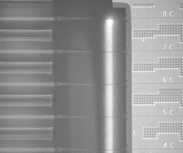
Fig. 8 – Microscope image of a photonic wire bond connection between an SOI chip and a single mode fiber array
Development and testing of algorithms for digital reconstruction
A mathematical description of the signals throughout the photonic ADC system, including distinction among time-invariant and time-variant signal impairments has been made by KIT. A system calibration process for retrieving the time-invariant part of the system transfer function was conceived and tested, based on the use of a highly stable optical pulse source. The further step was to estimate and compensate the time-variant impairments by using the spectral overlap region between adjacent spectral slices from the measurement itself. DSP algorithms have been implemented to stitch all the slices, removing time delays and amplitude/phase imbalances between the slices.
Test of the DSP algorithms in a proof-of-concept down-scaled photonic ADC experiment has been performed by KIT, where an 80 GBaud QPSK signal was sliced into four 20 GHz slices with subsequent spectral stitching digitally to recover the original signal.
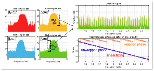
Fig. 10– Proof-of-concept experiment. (a) Four sliced spectrum of an 80 GBd QPSK signal. (b) Spectrum of the overlap region between slice 2 and slice 3. (c) wrapped phase (orange), unwrapped phase (blue) and linear fitting of the unwrapped phase (red) for the overlap region between slice 2 and slice 3.
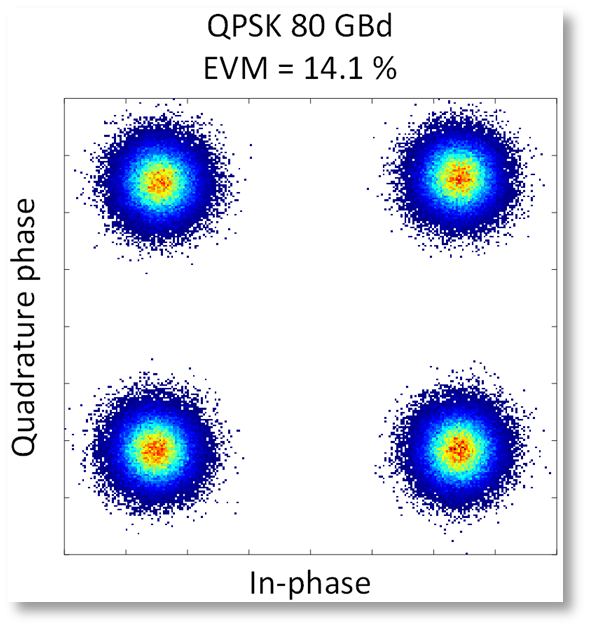
Fig. 11 – Constellation for the reconstructed 80GBaud data signal.
In addition to the spectrally sliced concept, in the course of the project a “non-sliced” optical arbitrary waveform measurement (OAWM) scheme has been adopted, which does not require optical slicing filters. The fundamental concept of the non-sliced OAWM system is illustrated in Figure 12. The scheme combines a chip-scale frequency comb generator, with a receiver system, that does not include any slicing filters and that is thus amenable to implementation on state-of-the-art high index contrast integration platforms such as silicon photonics. The incoming optical arbitrary waveform with Fourier spectrum is split into copies, which are routed to an array of IQ receivers, labeled by subscripts . The IQ receivers are also fed with time-delayed copies (delays ) of the LO comb, which consists of M tones with complex amplitudes at optical frequencies , separated by the free spectral range (FSR) of the comb,
(1)
The output signals of all IQ receivers are digitized by an array of analog-to-digital converters (ADC), and an estimate of the envelope of the arbitrary optical waveform is reconstructed by digital signal processing (DSP). Each IQ receiver (IQR) consists of a 90° optical hybrid (OH) and two pairs of balanced photodetectors (BPD) and is read out by two corresponding ADCs to obtain the in-phase component and the quadrature component of the respective baseband signal, see Inset 1 in Figure 12. All IQ receivers and ADCs have a bandwidth of within which the mixing products of the various LO tones with the respective adjacent parts of the signal spectrum can be detected. For simplicity, we assume that the overall transfer function for the in-phase and quadrature components are identical for each IQR ν, and that they have an ideal 90° phase relationship. In real systems, this is not necessarily the case, such that a more advanced system model is needed.
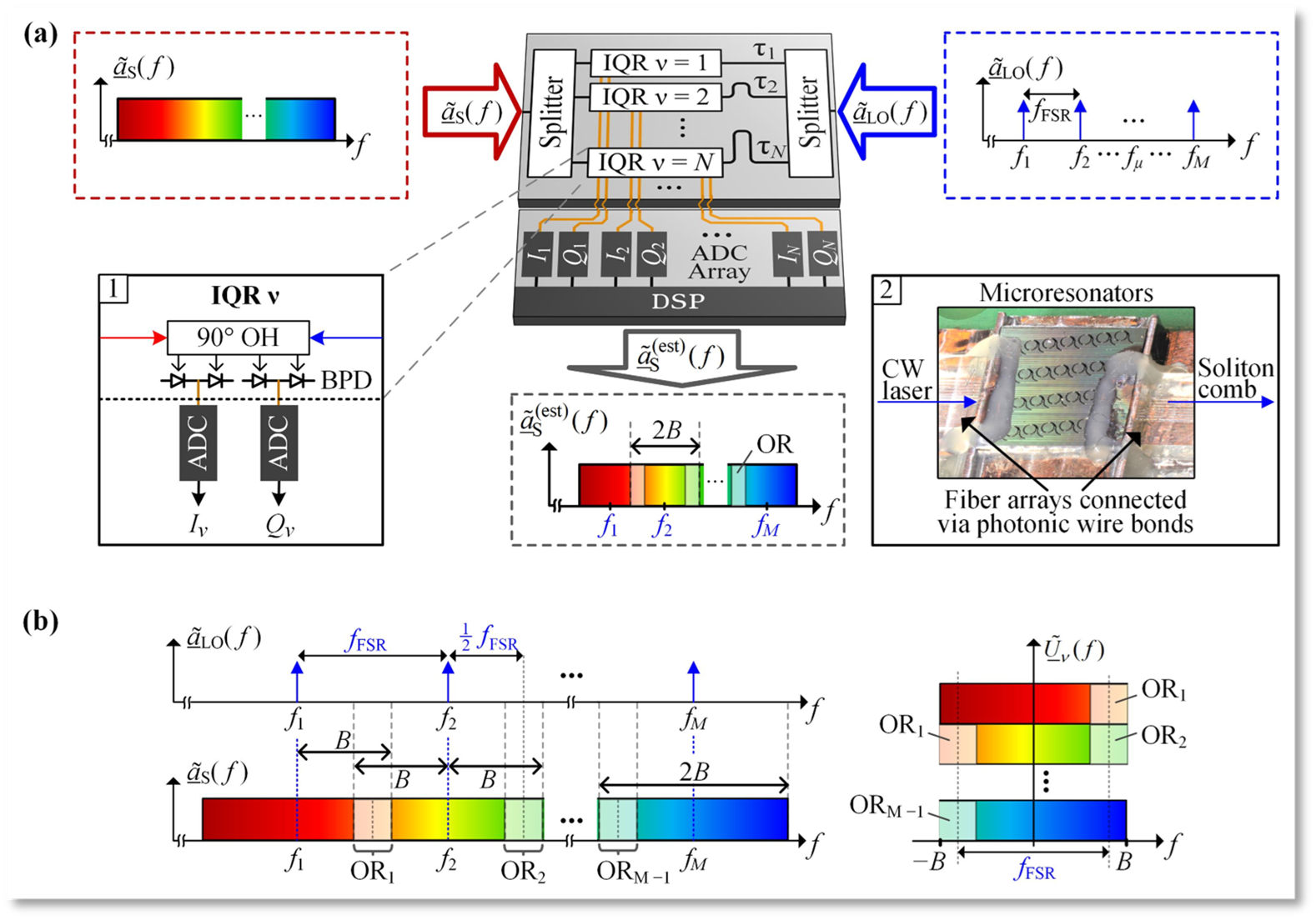
Fig. 12 – Concept of non-sliced optical arbitrary waveform measurement (OAWM) using a chip-scale frequency comb generator as a multi-wavelength LO. (a) The optical input signal with spectrum and the LO comb with spectrum are split into copies. The N copies of the LO comb, each comprising narrowband tones spaced by a free spectral range , are then delayed by distinct delays before being fed to in-phase and quadrature receivers (IQR), where they act as LO for coherent detection of the respective signal portion. The in-phase ( ) and quadrature ( ) outputs of the IQ receivers are read out by 2N corresponding analog-to-digital converters (ADC). Digital signal processing (DSP) is applied to recover an estimate of the optical input spectrum. Inset 1: Schematic of IQR ν with a 90° optical hybrid (OH), a pair of balanced photodetectors (BPD) and corresponding ADC (bandwidth ), providing the in-phase and quadrature components and of the respective baseband signals. Inset 2: Illustration of a chip-scale Kerr soliton comb source, comprising a continuous-wave pump laser and a high-Q Kerr-nonlinear microresonator. The comb free-spectral range typically is tens of GHz. (b) The composite baseband signals contain a superposition of the individual mixing products of each LO tone with the spectrally adjacent portion of the signal within a bandwidth B to either side of the respective LO tone Exploiting the fact that the various portions of the LO are subject to different time delays and that individual LO tones thus feature distinct phase differences, we can separate the superimposed mixing products by DSP.
Note that the receiver bandwidth is chosen slightly larger than half the FSR, leading to overlap regions (shaded stripes). Within these overlap regions, the same spectral portion of the signal is transferred to two distinct portions at the edges of the baseband signal spectrum close to . This leads to redundant information that can be used to estimate random phase drifts along the various detection paths.
Experimental demonstrators
The algorithms for spectral stitching have been developed and experimentally tested in a discrete device-based testbed, verifying their correct operation over a 400-GHz wide frequency range where four 80 GBaud QPSK signals had been placed in such a way to partly overlap two adjacent spectral slices each.
In the following of the project the experimental testbed for the first-generation photonic ADC testing, mainly based on discrete components, has been realized, successfully demonstrating the reconstruction of a 320-GHz wide frequency range including various complex modulation-based data signals. ENOB estimation was also performed, with the 2.3 value obtained mainly limited by the relatively low optical carrier-to-noise ratio of the employed optical comb. Results are reported by Fig. 13.
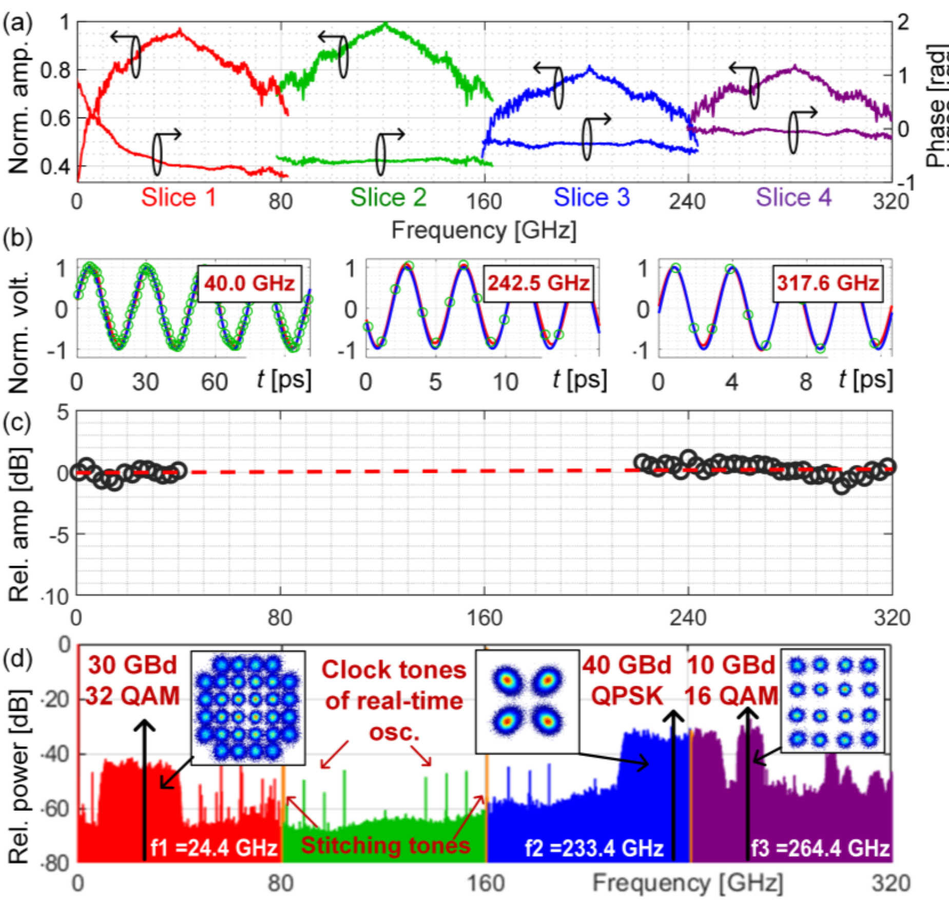
Fig 13 – Experimental results of the first-generation ADC demonstration.
A subsequent second-generation photonic ADC demonstration has been performed during the last part of the project, embedding all the packaged and integrated subsystems developed during the project, i.e. the multi-chip assembly of the optical spectrally-sliced IQ receiver array, the fiber-packaged microcomb generator and the fiber-packaged line-selection and flattening module. The reported demonstration excluded at first the electro-optic conversion stage consisting of the Mach-Zehnder modulator, demonstrating correct analog-to-digital conversion of an optical arbitrary waveform with total bandwidth occupation of 320 GHz verified through reconstruction of 3 signals carrying complex modulation formats across the analyzed frequency range. Results are shown in Fig. 14. The same sliced concept has been applied for preliminary demonstration of spread spectrum communications. Unfortunately, subsequent damage of the receiver assembly prevents further demonstrations including the electro-optical modulation stage.
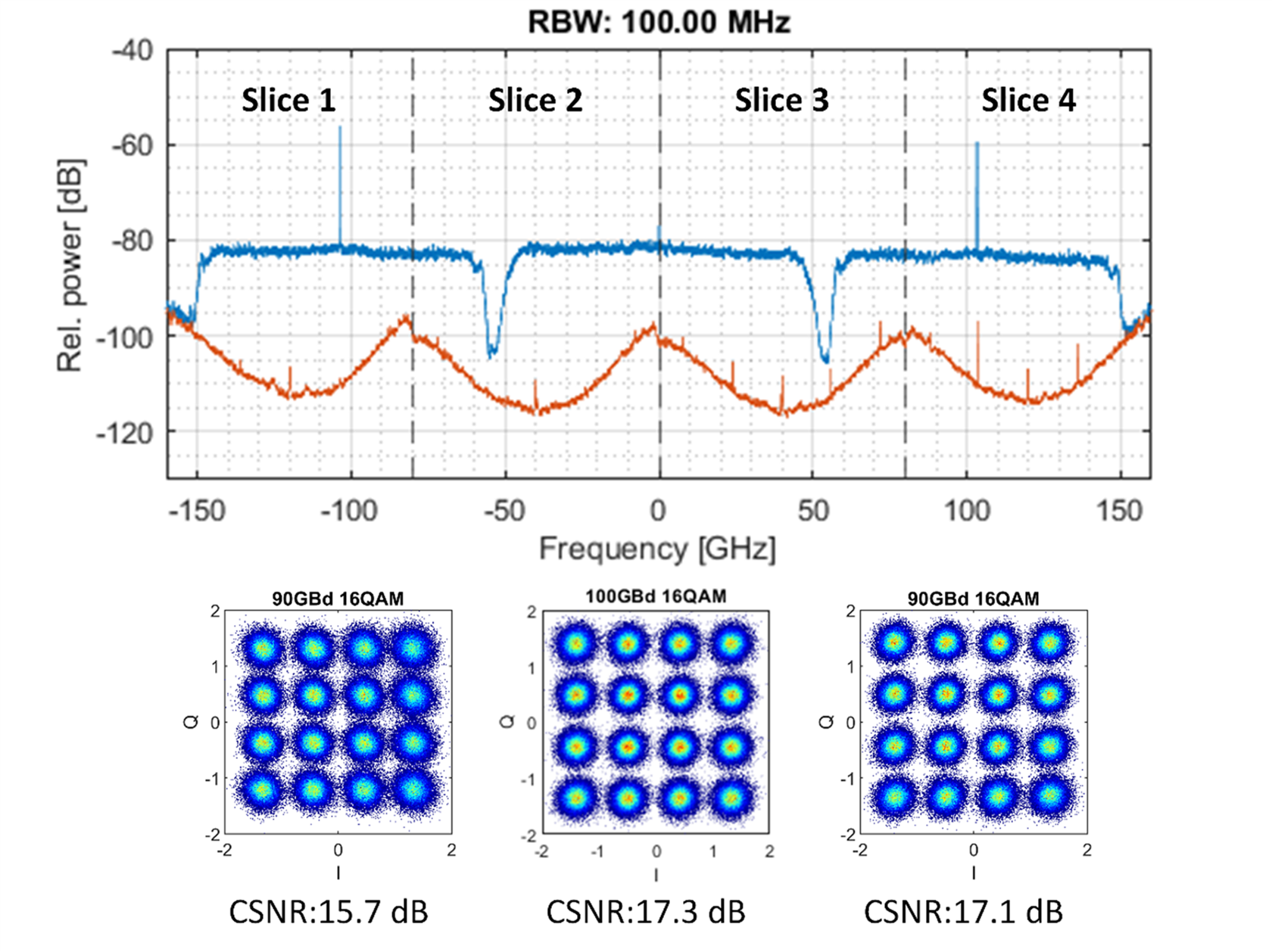
Fig 14 – Optical arbitrary waveform measurement based on the second-generation ADC system.
However, in parallel, an alternative approach which does not require to spectrally slice the signal spectrum in the optical domain has been conceived. Stitching algorithms for such a “non-sliced” approach have been developed and 610 GHz-wide optical arbitrary signal reconstruction has been experimentally validated. Results are reported in Fig. 15.
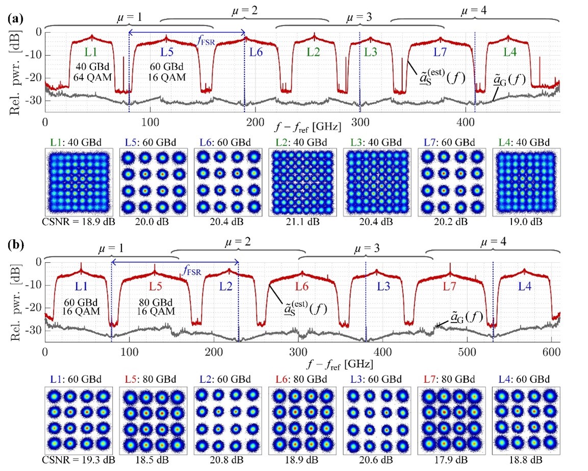
Fig 15 – 490GHz- and 610GHz-bandwidth optical arbitrary waveform measurement based on the non-sliced approach
References
[2] J. N. Kemal et al., “32QAM WDM transmission at 12 Tbit/s using a quantum-dash mode-locked laser diode (QD-MLLD) with external-cavity feedback,” Opt. Express, vol. 28, no. 16, pp. 23594–23608, Aug. 2020, doi: 10.1364/OE.392007.